
BJT stands for Bipolar Junction transistor. The BJT transistor is a three-layer and three-terminal semiconductor device. It is a three-terminal semiconductor device invented by William Shockley in Bell Labs. The basic aim while inventing BJT was to replace the giant vacuum tubes, which were previously been widely used for amplification purposes. Due to the size of the tubes, the devices were not possible to shrink their sizes. Almost every book of Basic or Advanced level electronics discusses BJT. It is the basic part of the curriculum of Electronics as well as Electrical technology.
The basic phenomena behind the transistor are to transfer the resistance. The basic meaning of the transistor is the transfer of the resistance. There are other types of transistors also available other than the BJT Transistor which are FET or Field-effect transistor, UJT or Uni-junction Transistor etc. But our main focus for today’s topic is the BJT Transistor which is Bipolar Junction Transistor in its full form.
What is BJT Transistor?
BJT transistor has the term “Bi-polar” in its name because the current in this transistor could flow due to both majority and minority charge carriers. The formation of the transistor is three layers of PNP or NPN semiconductor materials. This means either we can make the Transistor by sandwiching the P substance of semiconductor with N-type on both ends or by N-type semiconductor in between two layers of P-type semiconductor materials. The name of the three terminals of the transistors is “Base, Collector, and Emitter”. According to the formation type, the Transistor has two types called “NPN or PNP” according to the semiconductor formation in the BJT Transistor.
BJT Symbols
The BJT is a three-layer and three-terminal semiconductor component with two kinds of formations NPN or PNP. That’s why there are two types of symbols to identify the formation types. By identifying the correct formation type, one could clearly get the idea of majority and minority charge carriers in the BJT Transistor and get a clear picture of what could go under the hood. Here are the two symbols of both types of Transistors.
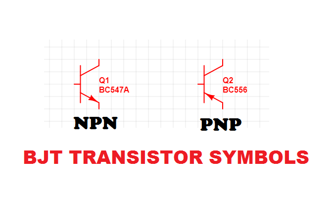
As you may see in the above figure that two terminals are on one side of the vertical bar and one terminal is on the other side of the verticle bar. The two terminals on the right side of the verticle bars are Collector and Emitter. The one terminal with the arrow is called the Emitter terminal of the BJT Transistor. The direction of the arrow indicates the formation type of the BJT Transistor. If the arrow points inwards to the verticle bar it means the transistor is the type of PNP. If the arrow points outwards the verticle bar it means the transistor is of type NPN. The single terminal on the left side of the verticle bar is known as the Base terminal. The remaining one is the Collector terminal.
